Rediscovered materials

Halide perovskites have significantly modified the landscape of materials for energy applications over the last decade. In particular, because of their impressive performances as absorbers in single junction solar cells or in Si/perovskite tandem solar cells [NREL chart]. Prior to that craze, the layered form of halide perovskites were the star of the family thanks to the great photophysical properties they exhibit. A large part of my work focus on the electronic, optical and transport properties of 3D, layered perovskites and parent compounds.

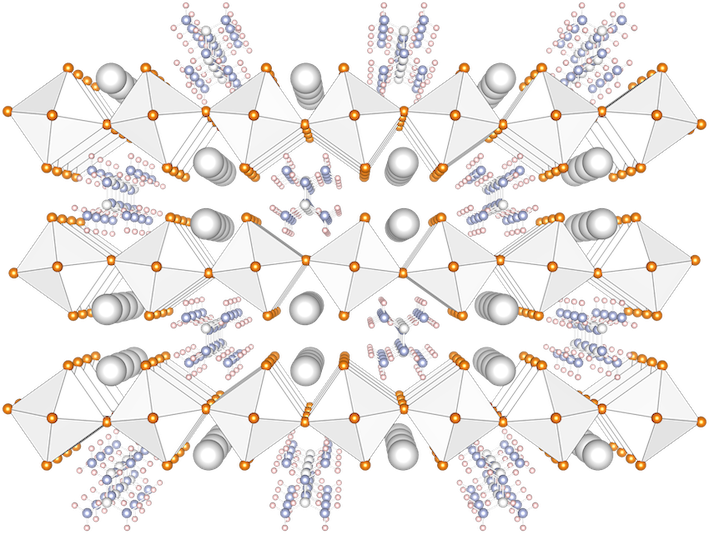
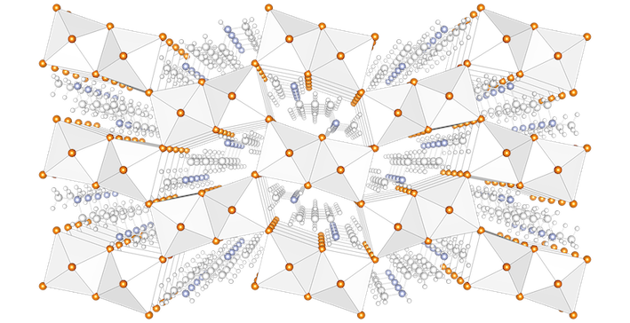
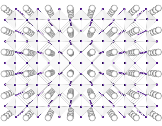
Tri-dimensional halide perovskites

We explored the electronic structure and spectroscopy of tri-dimensional (3D) halide perovskites, whether they are lead-based, e.g. FASnI3, or lead-free materials. The decisive role of surfaces and interfaces has been explored.

We also investigated the amount and effect of Rashba and Dresselhaus couplings in 3D halide perovskites.

Variations arond 3D materials, such as hollow perovskites or vacancy-ordered double perovskites, are also considered.

Layered halide perovskites

Most of our activity revolves around layered perovskites. We have investigated the composite nature of those 2D-like compounds marked by strong quantum and dielectric confinement, leading to strong electronic features.

We recently proposed a design of principle, based on the concept of lattice mismatch, to grow layered halide perovskites with thicker perovskite layers and controlled properties.

Parent compounds

The craze around halide perovskites has pushed for the reassessment of other materials also based on MX6 octahedra but not necessarily corner-shared. These perovskitoids have promising properties, either as lead-free alternatives to perovskites or for light-emission applications. Recently, we helped rationalized new type of materials based on diammonium cations and explored the potential of Ag/Bi halide double salts.